


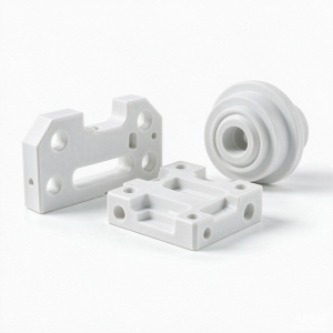
Ceramic substrates carry and insulate an electronic circuit. They are the base on which a conductor pattern is deposited, so the surface is the product.
Silicon nitride substrates are the choice for power modules that cycle hard, such as traction and automotive inverters. They combine usable conductivity with the 6-8 MPa·m½ toughness needed to survive thermal cycling on a copper bond.
Silicon nitride pairs high strength of 700-900 MPa with 6-8 MPa·m½ toughness at only 3.2 g/cm³. It survives the thermal shock that cracks most ceramics, resists molten non-ferrous metals, and its fine grain allows bearing-grade finishes.
It is among the more expensive options, and unlike SiC its thermal conductivity is a modest 25-35 W/m·K, so it is specified for mechanical reliability rather than heat spreading.
Specifications
| Thickness | 0.25-2.0 mm |
| Maximum size | up to 200×200 mm |
| Thickness tolerance | ±0.02 mm |
| Camber | under 0.1% of length |
| Surface finish | Ra 0.2-0.8 µm |
| Vias | drilled or laser cut, from 0.1 mm |
| Metallisation | thick film, thin film or DBC available |
Silicon Nitride Properties
| Composition | Gas-pressure sintered silicon nitride |
| Density | 3.20-3.25 g/cm³ |
| Vickers hardness | 1500-1600 HV |
| Flexural strength | 700-900 MPa |
| Fracture toughness | 6-8 MPa·m½ |
| Max. service temperature | 1000°C (1200°C short term) |
| Thermal conductivity | 25-35 W/m·K |
| Thermal expansion (20-1000°C) | 3.2 ×10⁻⁶/K |
Machining and Tolerances
Substrates are tape cast or rolled to thickness, fired, then lapped or ground to finished gauge. Vias are drilled or laser cut, and where a circuit needs it the surface is metallised with thick film, thin film or direct bonded copper before delivery.
Where It Is Used
- Power module and IGBT base plates
- LED and high-brightness die attach substrates
- RF and microwave circuit carriers
- Sensor and heater element bases
- Insulated metal substrate replacement in power conversion
Frequently Asked Questions
Which substrate material should I choose?
Alumina for general use and lowest cost, aluminium nitride where heat has to move, and silicon nitride where the circuit sees thermal cycling and mechanical load. We base the choice on heat flux and cycling duty rather than on conductivity alone.
Do you supply metallised substrates?
Yes. Thick film, thin film and direct bonded copper are available, and we can supply either the blank or the finished metallised panel depending on your process.